World's First "Quantum Semiconductor" Created by Scientists
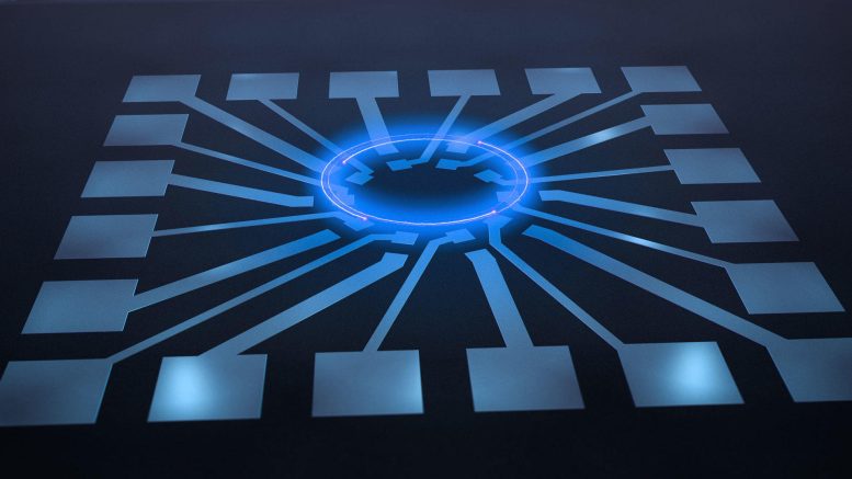
The first quantum semiconductor device to exhibit the topological skin effect has been successfully created. This device, wherein electrons (symbolized by a blue circle) flow along the edge, exhibits unparalled resilience despite deformations in the material or other external disruptions. This quantum semiconductor represents a significant advancement in the creation of minuscule topological electronic devices. Credit is due to Christoph Mäder/pixelwg.
Semiconductor devices, tiny components that regulate electron movement in modern electronic goods, are critical components in an extensive array of high-tech items, such as mobile phones, laptops, and car sensors, as well as advanced medical equipment. Nonetheless, material impurities or variations in temperature may hinder electron flow, leading to instability.
The Würzburg-Dresden Cluster of Excellence ct.qmat—Complexity and Topology in Quantum Matter, comprised of theoretical and experimental physicists, has now produced a semiconductor device made from aluminum-gallium-arsenide (AlGaAs). This device showcases a topological quantum phenomenon that protects its electron flow - typically vulnerable to disturbances. The exciting findings from this landmark research were recently published in the respected journal Nature Physics.
Professor Jeroen van den Brink, Director of the Institute for Theoretical Solid State Physics at the Leibniz Institute for Solid State and Materials Research in Dresden (IFW), and a principal investigator of ct.qmat, explains, “The topological skin effect ensures that currents between the different contacts on the quantum semiconductor remain undisturbed by impurities or other external perturbations. It eliminates the need for extremely high levels of material purity currently required in manufacturing electronics, making topological devices increasingly desirable within the semiconductor industry.”
Famed for their exceptional resilience, topological quantum materials are ideally suited for power-intensive applications. “Our quantum semiconductor marries stability with precision – a rare trait. This positions our topological device as a promising addition to sensor engineering,” says the team.
The team has used the topological skin effect to develop new types of high-performance electronic quantum devices that could be incredibly small. “Our topological quantum device has a diameter of around 0.1 millimeters and could be made even smaller,“ comments van den Brink. The team from Dresden and Würzburg's achievement is the first successful realization of the topological skin effect on a microscopic scale, in a semiconductor material. This quantum phenomenon was initially observed at macroscopic levels three years ago, but only in artificial metamaterials, not natural ones. This development is the first time a topological quantum device, which is robust yet ultra-sensitive, has been created using a minute semiconductor.
According to van den Brink, “In our quantum device, the current-voltage relationship is safeguarded by the topological skin effect because the electrons are confined to the edge. Even if there are impurities, the current flow remains stable.” He adds, “Furthermore, the contacts can detect the minutest changes in current or voltage. This makes the topological quantum device uniquely adept at producing high-precision sensors and amplifiers with extremely small diameters."
By cleverly configuring materials and contacts on the AlGaAs semiconductor device, the topological effect was induced under extreme cold conditions and a strong magnetic field. “We brought out the topological skin effect from the device,” explains van den Brink. The team employed a two-dimensional semiconductor structure wherein the electrical resistance could be measured at the contact edges, revealing the topological effect directly.
From 2019, ct.qmat has been studying topological quantum materials in Würzburg and Dresden, investigating their unusual behavior under extreme conditions such as ultra-low temperatures, high pressures, or strong magnetic fields.
This recent success is due to persistent collaboration between scientists in both locations. The new quantum device, developed at the IFW, was a product of cooperative efforts involving theoretical physicists from Universität Würzburg and both theoretical and experimental researchers in Dresden. Following its manufacture in France, the device was tested in Dresden. Van den Brink and his colleagues are now keenly focused on further research into this phenomenon, with the goal of harnessing it for forthcoming technological innovations.