Advancements in Transistors: Monolayer Black Phosphorus and Germanium Arsenide Based
January 6, 2024
Feature
This article has undergone a review in accordance with Science X's editorial process and policies. Key features highlighted by editors to assure the content's credibility include:
- fact-checked
- peer-reviewed publication
- trusted source
- proofread
Article by Ingrid Fadelli, Tech Xplore
Two-dimensional (2D) semiconductor materials show immense potential towards the development of advanced electronic devices, such as wearables and miniaturized electronics. Unlike their bulky counterparts, these materials retain carrier mobility despite reduced thickness.
Monolayer transistors, slimmer variants of critical electronic components that regulate and boost electrical current in most devices, have seldom been made from 2D semiconductors, despite their potential. Most monolayer transistors created using 2D semiconductors are made with few chosen materials with stable lattice structures like graphene, tungsten diselenide, and molybdenum disulfide (MoS2).
A team of researchers from Hunan University, the Chinese Academy of Sciences, and Wuhan University has made strides towards developing new monolayer transistors using other 2D semiconducting materials that have mainly been used to create multi-layer transistors, such as black phosphorus (BP) and germanium arsenide (GeAs). The team’s work is documented in the journal Nature Electronics.
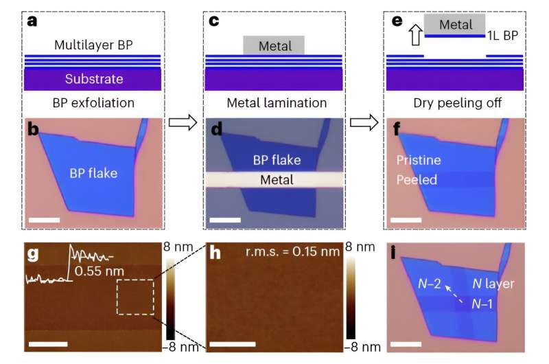
'Fabricating monolayer transistors from promising 2D materials such as black phosphorus and germanium arsenide is quite challenging as it is hard to form robust electrical contacts with these delicate 2D materials', researchers Wangying Li, Quanyang Tao, and their team mentioned in their research paper. 'We have demonstrated the fabrication of monolayer black phosphorus and germanium arsenide transistors with three-dimensional raised contacts using a van der Waals peeling technique.'
The key aim of this research was to formulate new transistors from monolayer 2D semiconductors that haven’t been used extensively in prior monolayer transistor designs. This poses several obstacles as some of these materials are tough to scale down uniformly without undermining their intrinsic properties.
To overcome this, the team designed a van der Waals (vdW) peeling technique that produces monolayer 2D transistors with 3D raised contacts. This procedure involves sticking flat metals onto multilayer 2D channels. Consequently, peeling off the metal removes the semiconductor layer on top.
The team utilized their proposed peeling method to construct homo-junctions and homo-superlattices from diverse 2D semiconductors such as BP, GeAs, InSe (indium selenide), and GaSe (gallium selenide).
They observed that the technique thinned down the channel part of their transistors while retaining the required thickness in the contact region.
'Upon using the technique, we assessed the electrical properties of the same 2D transistor with varying channel thicknesses. We discovered a significant drop in the carrier mobility of black phosphorus when reducing body thickness. This behaved more like a regular bulk semiconductor rather than a pure van der Waals semiconductor', Li, Tao, and their team noted.
In their most recent work, the researchers demonstrated the effectiveness of their technique in developing promising monolayer transistors with 3D-raised contacts based on BP and GeAs. The layer-by-layer peeling method proposed by the researchers could unlock new possibilities for the fabrication of thinner and scalable transistors using unusual 2D semiconductors, typically deemed poorly performing for these applications.
'The work has potential implications for other unstable monolayer materials beyond 2D semiconductors such as organic monolayers and perovskite monolayers, which have previously been considered to be non-conductive or to have poor intrinsic properties, but which are actually limited by the poor contact between the metal and monolayers,' Li, Tao and their colleagues added.
© 2024 Science X Network