Tiny Meron Lattices: Ideal Spin Injectors for LEDs at Millimeter Scale

July 31, 2023 feature
This article has been reviewed according to Science X's editorial process and policies. Editors have highlighted the following attributes while ensuring the content's credibility:
- fact-checked
- peer-reviewed publication
- trusted source
- proofread
by Ingrid Fadelli , Phys.org
Merons, topological structures based on in-plane magnetized magnetic materials, could have numerous valuable applications, particularly for carrying information or storing magnetic charge. Most past realizations of these structures, however, were limited in size and thermal stability or had impractical requirements, such as the application of external magnetic fields.
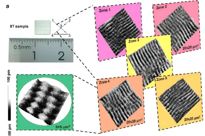
Researchers at Xiamen University and various other institutes in Japan, China, and Sweden recently designed large-scale meron lattices that could be used to inject spins in LEDs or other devices. These lattices, introduced in Nature Electronics, are comprised of three layers: a thin iron film sandwiched between a palladium and a magnesium oxide film.
'The use of topological spin structures is restricted by their limited scale, thermal stability or magnetic field requirements,' Yaping Wu, one of the researchers who carried out the study, told Phys.org. 'In this work, we developed a high-magnetic-field (HMF) -assisted growth approach to overcome these limitations, enabling the construction of millimeter-scale meron lattices that are stable at room temperature and zero-external magnetic field. We are then curious how would these lattices modulate electron-spin transport.'
Their theoretical analysis revealed the answer—the meron lattices are able to induce a spin polarization in the injected current. When used to inject spins in a nitride-based LED, the meron lattices created by Wu and her colleagues achieved very promising results, enabling a record high circularly polarized electroluminescence. Notably, this was attained at ambient, room temperature conditions, without requiring particularly low temperatures or the use of external magnetic fields.
'This research is based on the idea and previous research efforts that using growth magnetic field to improve the crystallization of materials,' Wu said. 'Meanwhile, our research group has been committed to the design, structural growth, and device development of wide-bandgap semiconductors. Therefore, the concept of combining the constructed millimeter-scale meron lattices with photoelectronic semiconductors was lighted in this work.'
Topological quasiparticles, such as merons or skyrmions, are essentially non-coplanar spin structures that are topologically protected inside magnetic materials. Wu and her colleagues set to design topological spin structures that are stable at room temperature and in the absence of an applied magnetic field, which so far proved very challenging.
'Topological stability relies on strong orbital interactions; thus, HMF during crystallization can enhance and freeze d-, s- and p-orbital couplings, just as we predicted through the first-principles calculations,' Wu explained. 'Accordingly, we designed and built equipment for an HMF-assisted molecular beam epitaxy (MBE) approach to grow strong-coupling materials.'
Using their proposed approach, the researchers created a trilayer structure , namely a palladium, an iron, and a magnesium oxide layer (Pd/Fe/MgO). This structure which enabled interfacial Dzyaloshinskii–Moriya interactions (DMI), was placed on a gallium nitride (GaN) wafer.
'The HMF was applied during the growth of the Fe film to further break the spatial inversion symmetry and control the orbital alignment to achieve highly ordered crystallization and spin. As a result, larger-scale meron lattices were constructed,' Wu said. 'The resulting large-scale meron lattices are stable at room temperature and under zero magnetic field.'
The large-scale meron lattices created by Wu and her colleagues can be used to transfer chirality from merons to electrons, and subsequently to photons. To test their performance, the researchers used the lattices as spin injectors for nitride-based LEDs, achieving a recording high circularly polarized electroluminescence of 22.5% at room temperature and under magnetic field of zero.
'We realized a large-scale meron lattice is the first constructed by the HMF-assisted MBE,' Wu said. 'The MBE system we developed can provides in situ magnetic fields up to 9 T. By growing the Pd/Fe/MgO trilayer under HMF, the DMI was dramatically enhanced.'
The recent work by Wu and her colleagues introduces a viable approach to modulate electron spins in topological spin structures. The team successfully applied this approach to their meron lattice, but it could eventually also be applied to other topological structures.
'We analyzed the topology-induced force (Fmeron) and the trajectory of electronspassing through the meron lattice,' Wu said. 'The meron lattice was capable of manipulating the transport of spin electrons with a theoretical limit of 50% in spin polarization. We also demonstrated a chirality transfer from meron lattices to electrons and then to photons.'
This team of researchers was the first to effectively integrate a meron lattice inside a semiconductor-based device, improving the device's performance. The design principle outlined in their paper could soon be used to create other topological structures that are stable at ambient conditions, without requiring an external magnetic field.
'Our HMF-assisted MBE approach effectively regulates strong-coupling materials by manipulating the orbital interactions,' Wu said. 'In our next studies, we will try to extend the application of this approach to achieve the customized growth of other crystals and topological spin structures such as large-scale skyrmions and vortices.'
© 2023 Science X Network


