Developing Compact Near-Sensor Computing Chips Through 3D Integration of 2D Materials

November 10, 2024 feature
This article has been reviewed according to Science X's editorial process and policies. Editors have highlighted the following attributes while ensuring the content's credibility:
fact-checked
peer-reviewed publication
trusted source
proofread
by Ingrid Fadelli , Tech Xplore
Three-dimensional (3D) integration has opened new possibilities for the development of denser circuits with more interconnected electronic components. 3D integration approaches entail stacking multiple layers of electronic circuits together, ultimately producing more compact and efficient devices.
These electronics fabrication strategies can reduce both the size and the power consumption of electronics while also boosting their performance. An emerging 3D integration approach that has been found to be particularly promising is monolithic 3D (M3D) integration, which involves the construction of transistors layer by layer on the same substrate instead of bonding individual chips together.
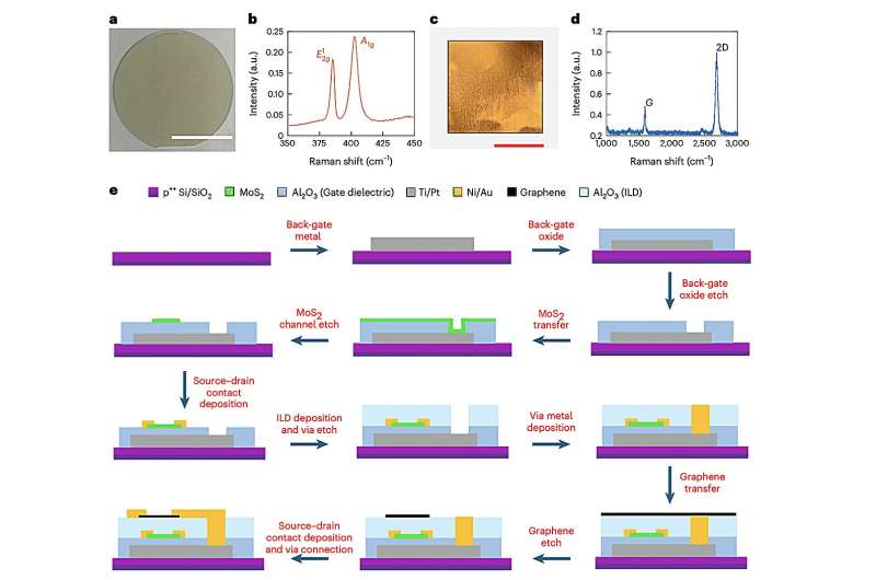
Researchers at Pennsylvania State University recently developed highly compact near-sensor computing chips via the heterogeneous M3D integration of two-dimensional (2D) materials. Their paper, published in Nature Electronics, demonstrates the fabrication of these chips using scalable strategies that are compatible with existing manufacturing processes.
'M3D integration is being increasingly adopted by the semiconductor industry as an alternative to traditional through-silicon via technology, as a way to increase the density of stacked, heterogenous electronic components,' Subir Ghosh, Yikai Zheng and their colleagues wrote in their paper. 'M3D integration can also provide transistor-level partitioning and material heterogeneity. However, there are few large-area demonstrations of M3D integration using non-silicon materials.'
As part of their recent study, Ghosh, Zheng and their colleagues set out to develop a sensing and near-sensor computing chip based on 2D electronics employing an M3D integration strategy. The chip they created integrates over 500 chemitransistors and over 500 memtransistors, with vertical interconnects (vias) that are 3 μm in size and at a 1 μm distance from each other.
'We report heterogeneous M3D integration of two-dimensional materials using a dense inter-via structure with an interconnect (I/O) density of 62,500 I/O per mm2,' Ghosh, Zheng and their colleagues wrote. 'Our M3D stack consists of graphene-based chemisensors in tier 2 and molybdenum disulfide (MoS2) memtransistor-based programmable circuits in tier 1, with more than 500 devices in each tier. Our process allows the physical proximity between sensors and computing elements to be reduced to 50 nm, providing reduced latency in near-sensor computing applications.'
A key advantage of the M3D integration approach employed by the researchers is that the entire fabrication process takes place at temperatures under 200 °C. This means it is compatible with back-end-of-line integration processes currently used to fabricate semiconductor-based devices.
As part of their study, Ghosh, Zheng and their colleagues used the computing chip they developed for chemical codification. Specifically, they developed an alert system that could be used to identify and classify different chemicals.
The chemitransistors in the team's chip were exposed to sugar solutions with different concentrations and the electrical signals they generated in response to these solutions were recorded. Subsequently, memtransistors processed the signals generated by the chemitransistors, converting them into analog and digital codes.
The findings of the team's alert system demonstrations highlight the potential of the new near-sensing computing chip for processing and classifying chemicals. In the future, their proposed fabrication approach could be scaled up to develop chips with an even greater number of circuits and sensors, which could tackle more advanced classification tasks.
More information: Subir Ghosh et al, Monolithic and heterogeneous three-dimensional integration of two-dimensional materials with high-density vias, Nature Electronics (2024). DOI: 10.1038/s41928-024-01251-8
© 2024 Science X Network


